Scientists take a 'spin' onto magnetoresistive RAM
Magnetoresistive random access memory (MRAM) is the forerunning candidate for the next generation digital technology. However, manipulating MRAM efficiently and effectively has been challenging. A revolutionary breakthrough was recently achieved by an interdisciplinary research team based at National Tsing Hua University (NTHU) in Taiwan, led by Prof. Chih-Huang Lai, Department of Materials Science and Engineering, and Prof. Hsiu-Hau Lin, Department of Physics. By adding a layer of platinum, only a few nanometers thick, it generates spin current to switch the pinned magnetic moments at will – a task that has never been accomplished before.
From mobile phones to computers, wearable devices, the Internet of Things, and smart city operations, data processing and storage are essential. To allow faster reading and writing, less power consumption and retaining data through a power outage, MRAM stands out in the keen competitions. Lai and Lin’s breakthrough, published in Nature Materials, adds wings to MRAM technology and attracts attentions from both industry and academy.
Steering spin currents in MRAM
At present, information processing in digital devices is mainly carried out using dynamic random access memory (DRAM), but it consumes significant power and faces serious hurdles when reduced in size.
DRAM utilizes the charges of electrons. “But, electrons have both charge and spin.” Lai said, “Why cannot one work with electron spins to manipulate MRAM?” To put the idea into practice, Lai and Lin formed an interdisciplinary research team with doctoral students Bohong Lin and Boyuan Yang.
Lin explained that the structure of MRAM is like a sandwich. The upper layer consists of a freely flipping magnet, in charge of data computation, while the bottom layer consists of a fixed magnet, responsible for data storage; and these two layers are separated by an oxide layer.
The challenge is to switch these layers of different natures by electrical means. After a long series of experiments, they found the key ingredient: a nanometer layer of platinum. Due to spin-orbit interactions, the electric current drives the collective motion of electron spins first. The spin current then switches the pinned magnetic moment effectively and precisely.
Spintronics blazing hot
In recent years, NTHU has been promoting cross-disciplinary cooperation, such as the MRAM research conducted by the materials expert Lai and the physicist Lin, who have learned to work together seamlessly.
Major international companies all participate in the competition of MRAM development, including TSMC, Intel, and Samsung. It’s likely that mass production of high-density MRAM will begin sometime this year, a development where the research team led by Lai and Lin has played a key role.
The research team is currently extending their groundbreaking discovery to other structures, and their ongoing findings are expected to have major impacts on the development of memory industry. In Lai’s view, the development of MRAM technology is going to have a decisive influence on the future growth and evolution of the world’s semiconductor industry.
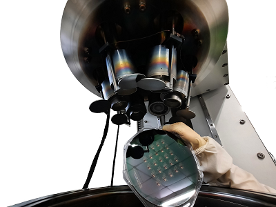
1. The sputtering technique has been widely used for thin film deposition. Under the sputtering guns, an eight-inch wafer with patterned device fabricated by deposition, photolithography, etching, etc. is shown.
2. A spin current (the yellow electric-like path) passes through the ferromagnetic (FM, blue region)/antiferromagnetic (AFM, red region) bilayer structure (the arrows mean the magnetic moment direction). The ferromagnetic moment and antiferromagnetic moment (the exchange bias) can both be switched (middle part: switching; upper part: already switched; lower part: to be switched).
References
Lin, P.-H.et al. Manipulating exchange bias by spin–orbit torque. Nat. Mater. 18, 335–341 (2019). https://doi.org/10.1038/s41563-019-0289-4