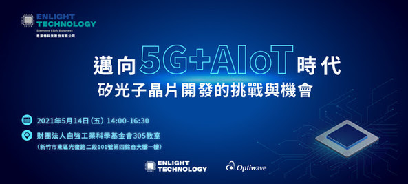
Enlight Technology – challenges and opportunities of silicon photonics wafer development – heading toward to 5G+AIoT new era

Enlight Technology – challenges and opportunities of silicon photonics wafer development – heading toward to 5G+AIoT new era
This class will discuss about the practical application of silicon photonics wafer, smart cards, sensors and 5G through Optiwave instances, in order to provide solution to the difficulties and challenges in research and design process, enhance the development of silicon photonics, and seize the commercial opportunities.
Time: 2021/5/14 (Fri) 14:00 - 16:30
Location: NTHU General Building Ⅳ 1F room 305
Target audience:
- Scholars, experts and graduate students with photoelectric, electrical, electronic, nano-engineering and micro-system backgrounds
- People who are relevant to chip design, optoelectronic technology, semiconductor technology and application.
|
Class schedule:
13:30~14:00 Check in
14:00~14:50 Challenges and opportunities of silicon photonics wafer
development in 5G+AIoT new era
Practical instances of silicon photonics wafer design process
- Electronic circuit simulation
- Optical circuit simulation
- Photoelectric coordinated circuit simulation
14:50~15:10 Break
15:10~16:00 Optoelectronic design and simulation from line level to system level
- Optoelectronic communication circuit design
- Photoelectric sensor circuit design
16:00~16:30 Q&A communication time
|
|||||||||||||
|
|||||||||||||
|
|||||||||||||
|

